Electron Microscopy: Principles, Evolution, and Advanced Imaging Techniques
An electron microscope is a powerful scientific instrument that uses a beam of electrons as its source of illumination rather than visible light. By utilizing electron optics—which function similarly to the glass lenses in a traditional light microscope—these devices can focus electron beams to produce highly magnified images or complex diffraction patterns.
The primary advantage of electron microscopy lies in resolution. Because the wavelength of an electron can be more than 100,000 times smaller than that of visible light, these microscopes can achieve a resolution of approximately 0.1 nm. In contrast, standard light microscopes are limited to a resolution of about 200 nm, making electron microscopy essential for observing the atomic and molecular structures of matter.
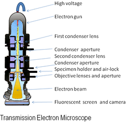
Key Facts

- Resolution: Reaches approximately 0.1 nm, far surpassing the 200 nm limit of optical microscopy.
- Illumination: Uses electron beams instead of photons (light).
- Core Types: Includes Transmission (TEM), Scanning (SEM), and Scanning Transmission (STEM) microscopes.
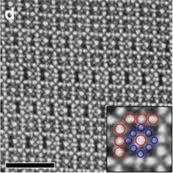
- Atomic Scale: Modern aberration-corrected instruments can image materials at the atomic level.
- Versatility: Used for everything from biological virions to nanocrystalline materials.
The Evolution of Electron Optics
The path to the modern electron microscope was paved by several key breakthroughs in physics. In 1883, Hertz demonstrated the manipulation of electron beams using a cathode-ray tube with electrostatic and magnetic deflection. This was followed by Emil Wiechert's work in 1899 on focusing electrons via axial magnetic fields and Arthur Wehnelt's 1905 improvement of oxide-coated cathodes to increase electron production.
A pivotal moment occurred in 1926 when Hans Busch developed the electromagnetic lens. By 1933, Ernst Ruska and Max Knoll constructed the first electron microscope that surpassed the resolution of optical microscopes.
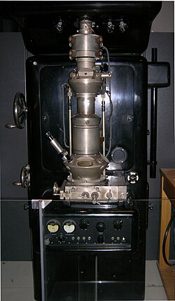
Commercialization followed quickly, with Siemens producing the first commercial model in 1938. Parallel developments occurred in North America during the 1930s at Washington State University and the University of Toronto. By 1937, Manfred von Ardenne had pioneered the scanning electron microscope (SEM), expanding the utility of the technology beyond simple transmission.
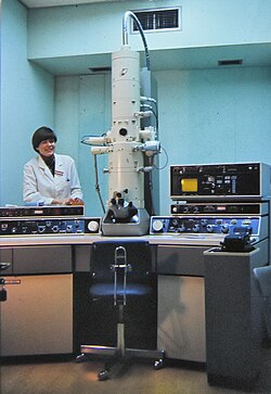
Throughout the mid-to-late 20th century, the field advanced rapidly. The 1940s saw the rise of high-resolution models, and by 1965, Albert Crewe introduced the scanning transmission electron microscope (STEM) using a field emission source. The 1980s brought the widespread adoption of field emission guns, which reduced chromatic aberrations and improved image coherence. The 21st century has been defined by aberration correction, allowing scientists to overcome previous optical limits and achieve unprecedented clarity.
Types of Electron Microscopes
![EDS spectrum of the mineral crust of the vent shrimp Rimicaris exoculata[63] Most of these peaks are K-alpha and K-beta lines. One peak is from the L shell of iron.](/images/cf/3f/cf3f3453482d160501321ff5597ddbf8d5c048838e29469ef16139ad05a0f895.png)
Depending on the sample thickness and the desired information, different types of electron microscopes are employed:
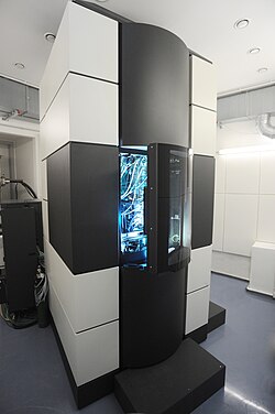
- Transmission Electron Microscope (TEM): Swift electrons pass through an ultra-thin sample to create an image.
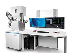
- Scanning Electron Microscope (SEM): Used for thicker samples; it scans the surface to provide detailed 3D-like topography.
- Scanning Transmission Electron Microscope (STEM): A hybrid that uses a scanned electron probe to pass through a sample.
- Electron Microprobe: Similar to an SEM but optimized specifically for chemical analysis.
- Low-Energy Electron Microscope (LEEM): Specialized for imaging the surfaces of materials.
- Photoemission Electron Microscope (PEEM): Similar to LEEM, but uses photons to emit electrons from a surface.
Aberration-Corrected Instruments
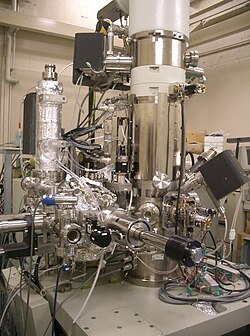
Historically, electron microscopes suffered from severe aberrations (distortions in the lens) that limited resolution. Around the turn of the century, the integration of computer-controlled lenses and alignment enabled the correction of these flaws. In 1998, Harald Rose and Maximilian Haider demonstrated aberration correction in TEM mode using a hexapole corrector, while Ondrej Krivanek and Niklas Dellby achieved it for STEM mode in 1999 using a quadrupole/octupole corrector.
Operating Modes and Analytical Techniques
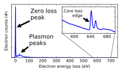
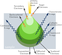
Electron microscopes do more than just take pictures; they act as analytical laboratories. By analyzing how electrons interact with matter, scientists can derive various types of data.
| Technique | Description | Primary Use |
|---|---|---|
| Secondary Electrons | Low-energy electrons emitted from the surface | Surface topography |
| Backscattered Electrons | High-energy electrons reflected back from the sample | Compositional contrast |
| EELS | Electron Energy Loss Spectroscopy | Chemical and electronic state analysis |
| EDS/WDXS | X-ray microanalysis | Elemental identification |
| CryoEM | Imaging of vitrified (frozen) samples | Biological structures/Viruses |
Specialized Imaging Methods
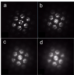
- Electron Diffraction: Used to determine the crystal structure of materials.
- Cathodoluminescence: Analyzing photons emitted as a result of the electron beam.
- Electron Tomography: Combining multiple 2D images to reconstruct a 3D volume.
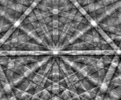
- EBSD (Electron Backscatter Diffraction): Typically used in SEMs to analyze crystallographic orientation.
Sample Preparation and Challenges
Preparing samples for electron microscopy is a rigorous process. For SEM, non-conductive samples are often coated in a thin layer of metal, such as gold, to prevent charging.

For TEM, samples must be sliced incredibly thin to allow electrons to pass through. Biological samples often require CryoEM techniques, where they are frozen rapidly (vitrified) to preserve their natural state without the need for chemical fixatives that might distort the structure.
![Pleolipoviral virion (HRPV-6)[71]](/images/ab/ee/abee79857cd4e465c74aa0f762ffc40cc43c974bf3c2cb78cce84eb416b23ad0.jpg)
Frequently Asked Questions
What is the main difference between SEM and TEM?
The primary difference is how the electrons interact with the sample. In TEM, electrons pass through a very thin specimen to create an image of its internal structure. In SEM, the electron beam scans the surface of a thicker specimen, providing a detailed image of its external topography.
Why is aberration correction important?
Aberrations are imperfections in the electromagnetic lenses that blur the image. Aberration correction uses specialized optical components and computer control to eliminate these distortions, allowing the microscope to reach its theoretical resolution limit and image individual atoms.
What is CryoEM and why is it used for biological samples?
Cryo-electron microscopy (CryoEM) involves flash-freezing samples in a vitrified state. This is used for biological specimens because it preserves their native structure and protects them from the vacuum of the microscope and the damaging effects of the electron beam.
How does an electron microscope achieve higher resolution than a light microscope?
Resolution is limited by the wavelength of the illumination source. Electrons have a significantly shorter wavelength than visible light photons—over 100,000 times shorter—which allows them to resolve much smaller features, down to approximately 0.1 nm.